Image is for your reference only,please check specifications for details
- SN75LVDS83B - TI
-
Manufacturer:TI
-
ManyChip's Part#:MC248970906
-
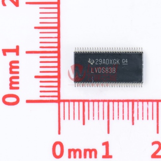
Package:TSSOP-56
-
Datasheet:Datasheet 3D Model
-
Description:The SN75LVDS83B FlatLink transmitter contains four 7Bit parallel-load serial-out shift registers, a 7X clock synthesizer, and five Low-Voltage Differential Signaling (LVDS) line drivers in a single integrated circuit
-
Stock Locations:
-
Availability:292 pcs In Stock
-
MOQ:1 pcs
-
Unit Price:$ 0
Updated at 18/06/2026 10:30:15(UTC+8)
Certifications
ManyChip is committed to product quality and safety with ISO 9001, ISO 13485, ISO 45001, UL, RoHS, CQC and REACH certifications.
Description
- The SN75LVDS83B FlatLink™ transmitter contains four 7-bit parallel-load serial-out shift registers, a 7X clock synthesizer, and five Low-Voltage Differential Signaling (LVDS) line drivers in a single integrated circuit. These functions allow 28 bits of single-ended LVTTL data to be synchronously transmitted over five balanced-pair conductors for receipt by a compatible receiver, such as the SN75LVDS82 and LCD panels with integrated LVDS receiver.
- When transmitting, data bits D0 through D27 are each loaded into registers upon the edge of the input clock signal (CLKIN). The rising or falling edge of the clock can be selected via the clock select (CLKSEL) pin. The frequency of CLKIN is multiplied seven times, and then used to unload the data registers in 7-bit slices and serially. The four serial streams and a phase-locked clock (CLKOUT) are then output to LVDS output drivers. The frequency of CLKOUT is the same as the input clock, CLKIN.
- The SN75LVDS83B requires no external components and little or no control. The data bus appears the same at the input to the transmitter and output of the receiver with the data transmission transparent to the user(s). The only user intervention is selecting a clock rising edge by inputting a high level to CLKSEL or a falling edge with a low-level input, and the possible use of the Shutdown/Clear (SHTDN). SHTDN is an active-low input to inhibit the clock, and shut off the LVDS output drivers for lower power consumption. A low-level on this signal clears all internal registers to a low-level.
- The SN75LVDS83B is characterized for operation over ambient air temperatures of 10°C to 70°C.
- Alternative device option: The SN75LVDS83A (SLLS980) is an alternative to the SN75LVDS83B for clock frequency range of 10MHz-100MHz only. The SN75LVDS83A is available in the TSSOP package option only.
- LVDS Display Series Interfaces Directly to LCD
- Display Panels With Integrated LVDS
- Package Options: 4.5-mm × 7-mm BGA,
- and 8.1-mm × 14-mm TSSOP
- 1.8-V Up to 3.3-V Tolerant Data Inputs to Connect
- Directly to Low-Power, Low-Voltage Application and
- Graphic Processors
- Transfer Rate up to 135 Mpps (Mega Pixel Per Second);
- Pixel Clock Frequency Range 10 MHz to 135 MHz
- Suited for Display Resolutions Ranging From HVGA
- up to HD With Low EMI
- Operates From a Single 3.3-V Supply and 170 mW (Typ.)
- at 75 MHz
- 28 Data Channels Plus Clock in Low-Voltage TTL to 4
- Data Channels Plus Clock Out Low-Voltage Differential
- Consumes Less Than 1 mW When Disabled
- Selectable Rising or Falling Clock Edge Triggered
- Inputs
- ESD: 5-kV HBM
- Support Spread Spectrum Clocking (SSC)
- Compatible with all OMAP™ 2x, OMAP™ 3x, and
- DaVinci™ Application Processors
SN75LVDS83B Specifications
| Attribute | Attribute Value |
|---|---|
| Datasheet | Datasheet |
| 3D Model | 3D Model |
| Mounting Style | Surface Mount |
| Case/Package | TSSOP-56 |
| Show | |
| Product Lifecycle Status | |
| RoHS | RoHS Compliant |
| Lead-Free Status | Lead Free |
Order guide
-
TT in advance (bank transfer), Western Union, Credit card,
PayPal. Customer is responsible for shipping fee, bank
charges, duties and taxes.
-
- You can choose whether shipping charges will be charged through your shipping account or by us.
- Please confirm with the logistics company in advance for remote areas.
(Additional charges ($35-$50) may apply for delivery in these areas)
- Delivery date: usually 2 to 7 working days.
- A tracking number will be sent after your order ships.
- - Carefully inspected and packed by ManyChip warehouse - Vacuum packaging - Anti-static packaging - Shockproof foam
- The terms here are for reference only, the actual terms are subject to the sales quotation. - Please confirm product specifications when ordering. - MOQ refers to the minimum order quantity required to purchase each part. - If you have special ordering instructions, please indicate them on the ordering page. - Inspection (PSI) will be performed prior to shipment.
- - Income Quality Control (IQC), 1000+ qualified dealers. - Chips are tested by authoritative organizations to ensure the quality, authenticity and safety of your device. - Decapsulation control - X-ray control - XRF inspection - Electrical testing - Surface testing -Digital components warehouse, covering an area of 800 square meters, with constant temperature and humidity
Contact Us
If you have any problem,please email to sales@manychip.com, we will response as soon as possisble.
Popular Search Parts
- Recommended Parts
- Hot Parts
- Popular Parts
- Recently Popular Parts
- TJA1044GTKZ DP83867ERGZT TPS1H000AQDGNRQ1 BLM18PG121SN1 BNX024H01 TFP410MPAPREP SN74LVC1G00DCKT TXS0102DCTT MPZ2012S102ATD25 DP83867IRRGZR
- FT245RL FT4232H MINI MODULE SN74LVC1G3157DCKR SN74AVC2T245RSWR SN74LVC1G125DBVR SN74LVC1G125DCKR TMS320F28335PGFA NCP15XH103F03RC SN74LVC1T45DCKR SN74LVC2G17DBVR
- 152001 101001 221010 350400 2N2646 SIM808 PC817C DL160 PTF08A BMI270
- SFH690ABT 140656 140595 MS27467T17B35P 3034426 MC33039P MC14526BCP MC74HC14AD NE5517D MC14551BCP
SN:H0.3LO61964V61Q0QC0S1
Buy SN75LVDS83B
Please fill the information below to send RFQ quickly,and we will respond immediately.