Image is for your reference only,please check specifications for details
Updated at 18/06/2026 10:30:15(UTC+8)
Certifications
ManyChip is committed to product quality and safety with ISO 9001, ISO 13485, ISO 45001, UL, RoHS, CQC and REACH certifications.
Description
- Product Details
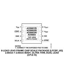
- The AD5683R/AD5682R/AD5681R/AD5683, members of the nanoDAC+® family, are low power, single-channel, 16-/14-/12-bit buffered voltage out digital-to-analog converters (DACs). The devices, except the AD5683, include an enabled by default internal 2.5 V reference, offering 2 ppm/°C drift. The output span can be programmed to be 0 V to VREF or 0 V to 2 × VREF. All devices operate from a single 2.7 V to 5.5 V supply and are guaranteed monotonic by design. The devices are available in a 2.00 mm × 2.00 mm, 8-lead LFCSP or a 10-lead MSOP.
- The internal power-on reset circuit ensures that the DAC register is written to zero scale at power-up while the internal output buffer is configured in normal mode. The AD5683R/AD5682R/AD5681R/AD5683 contain a power-down mode that reduces the current consumption of the device to 2 µA (maximum) at 5 V and provides software selectable output loads while in power-down mode.
- The AD5683R/AD5682R/AD5681R/AD5683 use a versatile 3-wire serial interface that operates at clock rates of up to 50 MHz. Some devices also include asynchronous RESET pin and VLOGIC pin options, allowing 1.8 V compatibility
- Product Highlights
- 1. High Relative Accuracy (INL).
- AD5683R/AD5683 (16-bit): ±2 LSB maximum.
- 2. Low Drift, 2.5 V On-Chip Reference.
- 2 ppm/°C typical temperature coefficient.
- 5 ppm/°C maximum temperature coefficient.
- 3. Two Package Options.
- 2.00 mm × 2.00 mm, 8-lead LFCSP.
- 10-lead MSOP.
- Applications
- Process controls
- Data acquisition systems
- Digital gain and offset adjustment
- Programmable voltage sources
- ### Features and Benefits
- Ultrasmall package: 2 mm × 2 mm, 8-lead LFCSP
- High relative accuracy (INL): ±2 LSB maximum at 16 bits
- AD5683
- External reference only
- Selectable span output: VREF or 2 × VREF
- Total unadjusted error (TUE): 0.06% of FSR maximum
- Offset error: ±1.5 mV maximum
- Gain error: ±0.05% of FSR maximum
- Low glitch: 0.1 nV-sec
- High drive capability: 20 mA
- Low power: 1.2 mW at 3.3 V
- Independent logic supply: 1.62 V logic compatible
- Wide operating temperature range: −40°C to +105°C
- Robust 4 kV HBM ESD protection
AD5683 Specifications
| Attribute | Attribute Value |
|---|---|
| Datasheet | Datasheet |
| 3D Model | 3D Model |
| Show | |
| Product Lifecycle Status | Recommended for New Designs |
Order guide
-
TT in advance (bank transfer), Western Union, Credit card,
PayPal. Customer is responsible for shipping fee, bank
charges, duties and taxes.
-
- You can choose whether shipping charges will be charged through your shipping account or by us.
- Please confirm with the logistics company in advance for remote areas.
(Additional charges ($35-$50) may apply for delivery in these areas)
- Delivery date: usually 2 to 7 working days.
- A tracking number will be sent after your order ships.
- - Carefully inspected and packed by ManyChip warehouse - Vacuum packaging - Anti-static packaging - Shockproof foam
- The terms here are for reference only, the actual terms are subject to the sales quotation. - Please confirm product specifications when ordering. - MOQ refers to the minimum order quantity required to purchase each part. - If you have special ordering instructions, please indicate them on the ordering page. - Inspection (PSI) will be performed prior to shipment.
- - Income Quality Control (IQC), 1000+ qualified dealers. - Chips are tested by authoritative organizations to ensure the quality, authenticity and safety of your device. - Decapsulation control - X-ray control - XRF inspection - Electrical testing - Surface testing -Digital components warehouse, covering an area of 800 square meters, with constant temperature and humidity
Contact Us
If you have any problem,please email to sales@manychip.com, we will response as soon as possisble.
Popular Search Parts
- Recommended Parts
- Hot Parts
- Popular Parts
- Recently Popular Parts
- MPZ2012S601A TPS7A39 DLP11SN900HL2 SN6505ADBVT BLM21PG600SN1 SBAS16LT1G NRVTS260ESFT1G ADXRS300ABG TPS3808G09DBVT AM26LV32EMDREP
- HD74LS04P RXM4AB1B7 FLASHPRO5 MPX5700AP HD74LS08P MJE15032G MD1803DFX TB6560AHQ L3G4200D ZB4BZ105
- TA7291S 1S1555 100056 TLP155E 2905340 2905470 2SD525 2SB554 2907919 BCM89811B1AWMLG
- 1735963 1716001 819550 RTK0EM0006S01212BJ 2EDN8524F TLV62568PDDCT LTM8068IY LMG1205YFXT THVD1451D ISO7762DWR
SN:H0.11667LO19923V70Q0QC0S0
Buy AD5683
Please fill the information below to send RFQ quickly,and we will respond immediately.