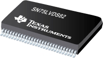

Image is for your reference only,please check specifications for details
- SN75LVDS82 - TI
-
Manufacturer:TI
-
ManyChip's Part#:MC270360796
-
Package:TSSOP-56
-
Datasheet:Datasheet 3D Model
-
Description:The SN75LVDS82 FlatLink™ receiver contains four serial-in, 7Bit parallel-out shift registers, a 7× clock synthesizer, and five low-voltage differential signaling (LVDS) line receivers in a single integrated circuit
-
Stock Locations:
-
Availability:256 pcs In Stock
-
MOQ:1 pcs
-
Unit Price:$ 0
Updated at 03/05/2026 10:30:15(UTC+8)
Certifications
ManyChip is committed to product quality and safety with ISO 9001, ISO 13485, ISO 45001, UL, RoHS, CQC and REACH certifications.
Description
- The SN75LVDS82 FlatLink™ receiver contains four serial-in, 7-bit parallel-out shift registers, a 7× clock synthesizer, and five low-voltage differential signaling (LVDS) line receivers in a single integrated circuit.
- These functions allow receipt of synchronous data from a compatible transmitter, such as the SN75LVDS83B, over five balanced-pair conductors, and expansion to 28 bits of single-ended low-voltage TTL (LVTTL) synchronous data at a lower transfer rate. The SN75LVDS82 can also be used with the SN75LVDS84 for 21-bit transfers.
- When receiving, the high-speed LVDS data is received and loaded into registers at the rate of seven times (7×) the LVDS input clock (CLKIN). The data is then unloaded to a 28-bit-wide LVTTL parallel bus at the CLKIN rate. A phase-locked loop (PLL) clock synthesizer circuit generates a 7× clock for internal clocking and an output clock for the expanded data. The SN75LVDS82 presents valid data on the falling edge of the output clock (CLKOUT).
- The SN75LVDS82 requires only five line-termination resistors for the differential inputs and little or no control. The data bus appears the same at the input to the transmitter and output of the receiver with the data transmission transparent to the user.
- The only possible user intervention is the use of the shutdown/clear (SHTDN) active-low input to inhibit the clock and shut off the LVDS receivers for lower power consumption. A low-level on SHTDN clears all internal registers to a low level and places the TTL outputs in a high-impedance state.
- The SN75LVDS82 is characterized for operation over ambient air temperatures of 0°C to 70°C.
- 4:28 Data Channel Expansion at up to 1904 Mbps Throughput
- Suited for SVGA, XGA, or SXGA Display Data Transmission From Controller to Display With Very Low EMI
- Four Data Channels and Clock Low-Voltage Differential Channels In and 28 Data and Clock Low-Voltage TTL Channels Out
- Operates From a Single 3.3-V Supply With 250 mW (Typical)
- 5-V Tolerant SHTDN Input
- Falling Clock-Edge-Triggered Outputs
- Packaged in Thin Shrink Small-Outline Package (TSSOP) With 20-Mil Terminal Pitch
- Consumes Less Than 1 mW When Disabled
- Pixel Clock Frequency Range of 31 MHz to 68 MHz
- No External Components Required for PLL
- Inputs Meet or Exceed the Requirements of ANSI EIA/TIA-644 Standard
SN75LVDS82 Specifications
| Attribute | Attribute Value |
|---|---|
| Datasheet | Datasheet |
| 3D Model | 3D Model |
| Mounting Style | Surface Mount |
| Case/Package | TSSOP-56 |
| Show | |
| Product Lifecycle Status | |
| RoHS | RoHS Compliant |
| Lead-Free Status | Lead Free |
Order guide
-
TT in advance (bank transfer), Western Union, Credit card,
PayPal. Customer is responsible for shipping fee, bank
charges, duties and taxes.
-
- You can choose whether shipping charges will be charged through your shipping account or by us.
- Please confirm with the logistics company in advance for remote areas.
(Additional charges ($35-$50) may apply for delivery in these areas)
- Delivery date: usually 2 to 7 working days.
- A tracking number will be sent after your order ships.
- - Carefully inspected and packed by ManyChip warehouse - Vacuum packaging - Anti-static packaging - Shockproof foam
- The terms here are for reference only, the actual terms are subject to the sales quotation. - Please confirm product specifications when ordering. - MOQ refers to the minimum order quantity required to purchase each part. - If you have special ordering instructions, please indicate them on the ordering page. - Inspection (PSI) will be performed prior to shipment.
- - Income Quality Control (IQC), 1000+ qualified dealers. - Chips are tested by authoritative organizations to ensure the quality, authenticity and safety of your device. - Decapsulation control - X-ray control - XRF inspection - Electrical testing - Surface testing -Digital components warehouse, covering an area of 800 square meters, with constant temperature and humidity
Contact Us
If you have any problem,please email to sales@manychip.com, we will response as soon as possisble.
Popular Search Parts
- Recommended Parts
- Hot Parts
- Popular Parts
- Recently Popular Parts
- 9FGV0241AKLF F28388DZWTS BLM18AG102SN1 LMZM23601SILT UCC21530QDWKRQ1 BLM21PG331SN1 MPZ2012S601A TPS7A39 DLP11SN900HL2 SN6505ADBVT
- DLP11SN900HL2 SN6505ADBVT BLM21PG600SN1 SBAS16LT1G NRVTS260ESFT1G ADXRS300ABG TPS3808G09DBVT AM26LV32EMDREP TPD6S300RUKR OPI1264C
- TPS2121RUXR CD74HC194E DP83822IRHBR FDMS86163P ADM1278 NSYTRV42 TBD62083APG FXMAR2102L8X DS24B33+ MPZ1608S601ATA00
- ADM7170 DV0P2990 SN74LVC1G97DCKR TCA9535PWR RB521S30T1G STM32H753VIT6 MPZ1608S221ATA00 CSD19537Q3 SN74LV1T125DBVR STUSB4500QTR
SN:H0.28333LO32269V78Q0QC0S0
Buy SN75LVDS82
Please fill the information below to send RFQ quickly,and we will respond immediately.