Image is for your reference only,please check specifications for details
Updated at 18/06/2026 10:30:15(UTC+8)
Certifications
ManyChip is committed to product quality and safety with ISO 9001, ISO 13485, ISO 45001, UL, RoHS, CQC and REACH certifications.
Description
- Product Details
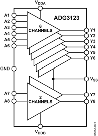
- The ADG3123 is an 8-channel, noninverting CMOS to high voltage level translator. Fabricated on an enhanced LC2MOS process, the device is capable of operating at high supply voltages while maintaining ultralow power consumption.
- The internal architecture of the device ensures compatibility with logic circuits running from supply voltages within the 2.3 V 5.5 V range. The voltages applied to Pin VDDA, Pin VDDB and Pin VSS set the logic levels available at the outputs on the Y side of the device. Pin VDDA and Pin VDDB set the high output level for Pin Y1 to Pin Y6 and for Pin Y7 to Pin Y8, respectively. The VSS pin sets the low output level for all channels. The ADG3123 can provide output voltages levels down to −24.2 V for a low input level and up to +35 V for a high input logic level. For proper operation, VDDB must always be greater than or equal to VDDA and the voltage between the Pin VSS and Pin VSS should not exceed 35 V.
- The low output impedance of the channels guarantees fast rise and fall times even for significant capacitive loads. This feature, combined with low propagation delay and low power consumption, makes the ADG3123 an ideal driver for TFT-LCD panel applications.
- The ADG3123 is guaranteed to operate over the −40°C to +85°C temperature range and is available in a compact, 20-lead TSSOP, Pb-free package.
- **Product Highlights**
- Compatible with a wide range of CMOS logic levels.
- High output voltage levels.
- Fast rise and fall times coupled with low propagation delay.
- Ultralow power consumption.
- Compact, 20-lead TSSOP, RoHS-compliant package.
- **Applications **
- Low Voltage to High Voltage Translation
- TFT-LCD Panels
- Piezoelectric Motor Drivers
- ### Features and Benefits
- 2.3 V to 5.5 V Input Voltage Range
- Output voltage levels (VDDA and VDDB to VSS ≤ 35 V)
- Low output voltage levels: down to −24.2 V
- High output voltage levels: up to +35 V
- Rise/fall Time: 12 ns/19.5 ns Typical
- Propagation Delay: 80 ns Typical
- Operating Frequency: 100 kHz Typical
- Ultralow Quiescent Current: 65 μA Typical
- 20 Lead, Pb-free, TSSOP Package
ADG3123 Specifications
| Attribute | Attribute Value |
|---|---|
| Datasheet | Datasheet |
| 3D Model | 3D Model |
| Show | |
| Product Lifecycle Status | Active |
Order guide
-
TT in advance (bank transfer), Western Union, Credit card,
PayPal. Customer is responsible for shipping fee, bank
charges, duties and taxes.
-
- You can choose whether shipping charges will be charged through your shipping account or by us.
- Please confirm with the logistics company in advance for remote areas.
(Additional charges ($35-$50) may apply for delivery in these areas)
- Delivery date: usually 2 to 7 working days.
- A tracking number will be sent after your order ships.
- - Carefully inspected and packed by ManyChip warehouse - Vacuum packaging - Anti-static packaging - Shockproof foam
- The terms here are for reference only, the actual terms are subject to the sales quotation. - Please confirm product specifications when ordering. - MOQ refers to the minimum order quantity required to purchase each part. - If you have special ordering instructions, please indicate them on the ordering page. - Inspection (PSI) will be performed prior to shipment.
- - Income Quality Control (IQC), 1000+ qualified dealers. - Chips are tested by authoritative organizations to ensure the quality, authenticity and safety of your device. - Decapsulation control - X-ray control - XRF inspection - Electrical testing - Surface testing -Digital components warehouse, covering an area of 800 square meters, with constant temperature and humidity
Contact Us
If you have any problem,please email to sales@manychip.com, we will response as soon as possisble.
Popular Search Parts
- Recommended Parts
- Hot Parts
- Popular Parts
- Recently Popular Parts
- BLM18EG221SN1 BLM18PG471SN1 BLM18SG121TN1 FXMA108 MAX3232EIDWR 1SS400SMFHT2R SZMMBZ5V6ALT1G MC78M05CDTRK SMMBT5401LT1G 10M04DCF256I7G
- LD1117S50TR CSD19505KCS TCA6424RGJR LD1117S33TR ATV12H055M2 ICE3BR1765J FSBB30CH60C DCA1000EVM IRL40SC209 LIS2DW12TR
- DCA1000EVM IRL40SC209 LIS2DW12TR MBRA340T3G MBR0540T1G SN754410NE 2N7002LT1G TDA8920BTH LME49720NA IRF3205PBF
- CD4052B LC1D50BD LC1D18E7 ABL8BPK24A12 TDA1220B 3025163 NCP1207A 1862466 2864273 NX5P3090UKZ
SN:H0.41172LO12099V61Q0QC0S0
Buy ADG3123
Please fill the information below to send RFQ quickly,and we will respond immediately.