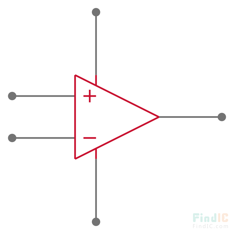

Image is for your reference only,please check specifications for details
- TLC27L4 - TI
-
Manufacturer:TI
-
ManyChip's Part#:MC167020166
-
Package:TSSOP-14
-
Datasheet:Datasheet 3D Model
-
Description:The TLC27L4 and TLC27L9 quad operational amplifiers combine a wide range of input offset voltage grades with low offset voltage drift, high input impedance, extremely low power, and high gain
-
Stock Locations:
-
Availability:239 pcs In Stock
-
MOQ:1 pcs
-
Unit Price:$ 0
Updated at 19/03/2026 10:30:15(UTC+8)
Certifications
ManyChip is committed to product quality and safety with ISO 9001, ISO 13485, ISO 45001, UL, RoHS, CQC and REACH certifications.
Description
- The TLC27L4 and TLC27L9 quad operational amplifiers combine a wide range of input offset voltage grades with low offset voltage drift, high input impedance, extremely low power, and high gain.
- These devices use Texas instruments silicon-gate LinCMOSTM technology, which provides offset voltage stability far exceeding the stability available with conventional metal-gate processes.
- The extremely high input impedance, low bias currents, and low-power consumption make these cost-effective devices ideal for high-gain, low- frequency, low-power applications. Four offset voltage grades are available (C-suffix and I-suffix types), ranging from the low-cost TLC27L4
- (10 mV) to the high-precision TLC27L9 (900 uV). These advantages, in combination with good common-mode rejection and supply voltage rejection, make these devices a good choice for new state-of-the-art designs as well as for upgrading existing designs.
- In general, many features associated with bipolar technology are available on LinCMOSTM operational amplifiers, without the power penalties of bipolar technology. General applications such as transducer interfacing, analog calculations, amplifier blocks, active filters, and signal buffering are easily designed with the TLC27L4 and TLC27L9. The devices also exhibit low voltage single-supply operation and ultra-low power consumption, making them ideally suited for remote and inaccessible battery-powered applications. The common-mode input voltage range includes the negative rail.
- A wide range of packaging options is available, including small-outline and chip-carrier versions for high-density system applications.
- The device inputs and outputs are designed to withstand -100-mA surge currents without sustaining latch-up.
- The TLC27L4 and TLC27L9 incorporate internal ESD-protection circuits that prevent functional failures at voltages up to 2000 V as tested under MIL-STD-883C, Method 3015.2; however, care should be exercised in handling these devices, as exposure to ESD may result in the degradation of the device parametric performance.
- The C-suffix devices are characterized for operation from 0°C to 70°C. The I-suffix devices are characterized for operation from -40°C to 85°C. The M-suffix devices are characterized for operation from -55°C to 125°C.
- The D package is available taped and reeled. Add R suffix to the device type (e.g., TLC27L9CDR).
- Trimmed Offset Voltage:
- TLC27L9...900 uV Max at 25°C,
- VDD = 5 V
- Input Offset Voltage Drift...Typically
- 0.1 uV/Month, Including the First 30 Days
- Wide Range of Supply Voltages Over
- Specified Temperature Range:
- 0°C to 70°C...3 V to 16 V
- -40°C to 85°C...4 V to 16 V
- -55°C to 125°C...4 V to 16 V
- Single-Supply Operation
- Common-Mode Input Voltage Range Extends Below the Negative Rail (C-Suffix, I-Suffix Types)
- Ultra-Low Power...Typically 195 uW
- at 25°C, VDD = 5 V
- Output Voltage Range includes Negative Rail
- High Input Impedance...1012 Typ
- ESD-Protection Circuitry
- Small-Outline Package Option Also Available in Tape and Reel
- Designed-In Latch-Up Immunity
- LinCMOS is a trademark of Texas Instruments Incorporated.
TLC27L4 Specifications
| Attribute | Attribute Value |
|---|---|
| Datasheet | Datasheet |
| 3D Model | 3D Model |
| Case/Package | TSSOP-14 |
| Show | |
| Product Lifecycle Status | |
| RoHS | RoHS Compliant |
| Lead-Free Status | Lead Free |
Order guide
-
TT in advance (bank transfer), Western Union, Credit card,
PayPal. Customer is responsible for shipping fee, bank
charges, duties and taxes.
-
- You can choose whether shipping charges will be charged through your shipping account or by us.
- Please confirm with the logistics company in advance for remote areas.
(Additional charges ($35-$50) may apply for delivery in these areas)
- Delivery date: usually 2 to 7 working days.
- A tracking number will be sent after your order ships.
- - Carefully inspected and packed by ManyChip warehouse - Vacuum packaging - Anti-static packaging - Shockproof foam
- The terms here are for reference only, the actual terms are subject to the sales quotation. - Please confirm product specifications when ordering. - MOQ refers to the minimum order quantity required to purchase each part. - If you have special ordering instructions, please indicate them on the ordering page. - Inspection (PSI) will be performed prior to shipment.
- - Income Quality Control (IQC), 1000+ qualified dealers. - Chips are tested by authoritative organizations to ensure the quality, authenticity and safety of your device. - Decapsulation control - X-ray control - XRF inspection - Electrical testing - Surface testing -Digital components warehouse, covering an area of 800 square meters, with constant temperature and humidity
Contact Us
If you have any problem,please email to sales@manychip.com, we will response as soon as possisble.
Popular Search Parts
- Recommended Parts
- Hot Parts
- Popular Parts
- Recently Popular Parts
- PMV16XNR VIPER06XN LM2596TVADJG TPD2E007DCKR MBR2H100SFT3G STL6P3LLH6 FSA2466UMX TLE8888QK MPZ1608S601ATD25 MIMX8MM6CVTKZAA
- MRF300AN TNY277GN IRFP4768 CD4026BE TOP244PN TDA7269A TOP256YN LIS3DHTR TOP250YN GV2MC02
- RSZE1S35M 2811446 RUMC21F7 XS508B1PAL2 NSYPFCR 1208021 1201578 TBD62003APG 402006 311605
- C315C222K2R5TA HMC557ALC4 STP4NK60ZFP NAU8814YG MC33172DR2G BA033FP TC4428EOA AD524SD IPG20N06S4L26ATMA1 AD5206BRUZ10
SN:H0.42128LO30498V51Q0QC0S1
Buy TLC27L4
Please fill the information below to send RFQ quickly,and we will respond immediately.